https://xellers.wordpress.com/electronics/1ghz-active-differential-probe/
Design and Simulation
The first order of business was to pick a topology and get it working in a SPICE simulation. Because Texas Instruments was kind enough to overnight free samples of a number of different high speed opamps, I decided to use TINA-TI, which is a free graphical front end for SPICE distributed by TI that includes built-in models for all of TI’s linear ICs. We were not supposed to do any design before the hackathon other than figuring out what non-standard parts we should bring. Therefore, a few days before the hackathon, I simply picked three different high speed opamps from TI that looked good, the THS3201, THS3202, and LMH6702, verified that their models looked OK in TINA-TI, and waited until the day of to decide which one to use and how to hook it up.
The first thing that becomes apparent when thinking about designing the differential amplifier is that a single opamp configured as a differential amplifier doesn’t make for a very good probe because there is a tradeoff between bandwidth and input impedance. The larger you make the gain-setting resistors, the higher the input impedance, but the feedback path is slowed down because the pole created by the feedback resistance and opamp input capacitance moves to the right when the feedback resistance is increased. To put that in more human terms, the feedback resistance and input capacitance form a lowpass filter, which slows down the opamp. Because we desire an extremely high input impedance, a single opamp is impractical. What can we do?
The textbook solution to the input impedance issue is to add an opamp buffer to each differential input channel, thus allowing the differential stage to have a low input impedance, which is seen by the high input impedance buffers instead of the input signal. This is the circuit you will mostly likely find if you search for “opamp differential amplifier”. Unfortunately, at high frequencies, we would really prefer not to use opamps where we don’t have to. Not only are high frequency opamps relatively expensive, incentivising us to use them sparingly, but the use of feedback also introduces stability issues.
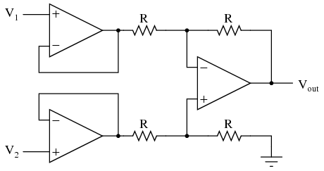
Vanilla-Flavored Differential Amplifier Schematic
In a high speed application, it is a poor choice to connect the output of an opamp directly to one of its inputs (as seen in a standard buffer circuit) because the input capacitance of the opamp will be driven directly by the output, reducing the phase margin and potentially resulting in oscillations. If you’re unfamiliar with those terms, the intuitive way to understand why this is a problem is to think about the phase shift introduced by the input capacitance of the opamp at high frequencies. This phase shift adds to the phase shift internal to the opamp (ideally an opamp transfer function will look approximately like a first order lowpass, with an extremely high DC gain) and the closer the overall phase shift at the maximum unity gain frequency is to -180 degrees, the closer the system is to a positive feedback oscillator, and the greater tendency it will have to overshoot and ring. The solution is to add a resistance into the feedback path, which tames the opamp’s output, but also slows it down. I tried this approach first, but was unable to simulate a buffered differential amplifier with satisfactory bandwidth (the target was 1GHz), so I moved on to a different approach, using a pair of MOSFET source followers without feedback as input buffers.
The best part of the source follower approach is that someone else had already designed a single-ended scope probe circuit with excellent bandwidth: the articlewas in a 2004 release of the Elektor magazine. I had also ordered several high speed MOSFETs and BJTs from Digikey before the hackathon, among which were several of the BF998 devices required to build the Elektor circuit (this was not an accident!). If I had more time, I would have liked to modify the design to include current source biasing of the MOSFETs to a negative supply rail in order to increase the input range and improve the linearity of the buffers. Realistically, however, this would add too much extra risk to a project that needed to be completed in only a day.
Here’s the Elektor circuit in LTSpice (because it appears TINA-TI can’t perform temperature sweeps). Note that I added a 200 ohm resistor in series with the input capacitor because it was resonating with the gate’s parasitic inductance, a 30 meg input resistor to boost the low frequency response, and a 2pF capacitor in parallel with the source resistor to squash a bump in the high frequency response.

Input Buffer Schematic
And here’s a Bode plot of the frequency response at 15, 25, and 35 degrees Celsius. There is some variation (about 0.2dB, or 1%, per 10 degrees C) in gain that might not be acceptable for a commercial grade probe, but adding temperature compensation would likely involve biasing the BF998 with some sort of PTAT current source, which was not feasible in the timeframe of the project.

Input Buffer Frequency Response at 15, 25, and 35 Degrees C
As you might notice from the Bode plot, an added advantage of the Elektor circuit is that is adds a 10x (20dB) attenuation, which means the differential amplifier sees low signal amplitudes and we can safely ignore “large signal” effects such as slew rate limiting. It’s also convenient as it increases the (likely limited) input range of whatever high speed scope we use. For example, the sampling heads on my Tektronix CSA803 scope have a maximum non-destructive input range of ±3V, which is unsuitable for scoping common 5V logic level signals. The final schematic of the probe’s amplifier circuitry in TINA-TI is shown below.
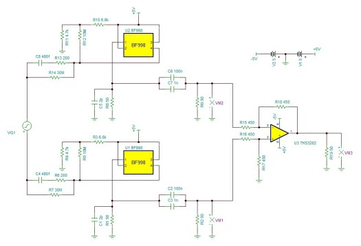
Schematic of the Analog Section
And here is a Bode plot of the differential input mode frequency response. The bandwidth looks pretty good! The phase response leaves something to be desired, but I considered it to be acceptable for the purposes of this project.
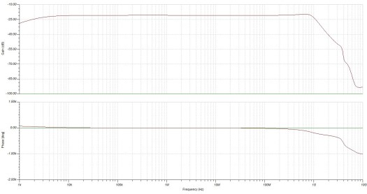
Differential Mode Bode Plot
I didn’t simulate the common mode response because the CMRR of the opamp is extremely high; the limitation to the CMRR in this circuit is due to gain mismatch between the two input buffers, which results from mismatch between the passive components in the signal path. This is not something that TINA-TI can simulate well because the tolerances on the components don’t necessarily reflect the maximum deviation we expect to see. Realistically, if two resistors or capacitors are part of the same batch of components and are next to each other on the same reel, then they will tend to be matched very well to each other, although their accuracy with respect to their rated value is still dictated by their tolerance.
Because we want the probe to be easy to use, the +5V and -5V power supplies need to be derived from a commonly-available power source. The most annoying “feature” of commercial active probes are the proprietary power connectors they integrate onto the BNC connector. What’s worse is that the design and pinouts of these connectors are poorly documented and change between generations of scopes from the same manufacturer (oh, and of course they’re incompatible between different scope manufacturers). It’s not just planned obsolescence, it’s forced obsolescence. What connector provides 5V at a reasonable current, is available everywhere on every reasonable electronic device, and is a global standard? USB! If we put a USB mini-B connector on our probe, that will always intuitively mean “connect me to power” to any end user.
In order to derive the -5V rail from USB power, a MAX1680 switched capacitor inverter was used. The datasheet suggests “opamp power rails” as an application of the chip, which I incorrectly assumed to mean that the output ripple at the chip’s rated current would be ignorable and I could just hook my opamp supply rail up to the output of the converter. As we learned later in the day, that was an incorrect assumption that we had to correct in the week 2 revision of the circuit.
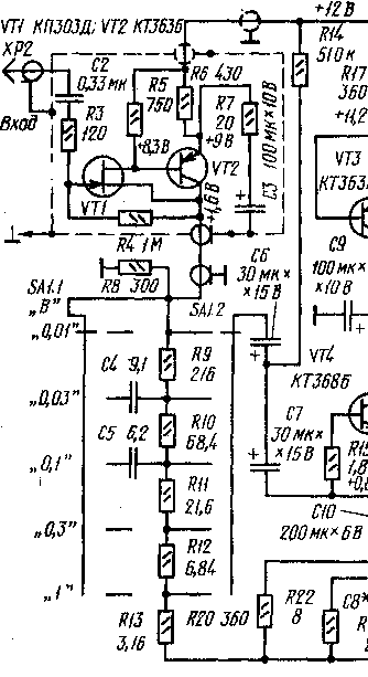
Смотри входные выносные пробники милливольтметров.
(Подборка "Вольтметр на операционном усилителе" - Измерения)
Милливольтметр
https://www.irls.narod.ru/izm/volt/volt06.htm
(до 30 Мгц)
Основная погрешность на частоте 20 кГц — не более ±2 %. Дополнительная частотная погрешность в интервале 100 Гц...10 МГц не превышает ±1, а в интервалах 20...100 Гц и 10...20 МГц — ±5 %. Погрешность от переключения пределов измерения в интервалах частот до 10 и от 10 до 20 МГц — соответственно не более ±2 и ±6 %. С достаточной для радиолюбительской практики точностью (±10...12%) прибором можно измерять напряжения частотой до 30 МГц, однако минимальное напряжение при этом составляет 3 мВ. Входное сопротивление милливольтметра — 1 МОм, входная емкость — 8 пФ.
Каскад выносного пробника охвачен 100 %-ной ООС. Его нагрузкой и одновременно элементом цепи ООС служит делитель напряжения R8—R13. Дополнительный резистор R8 включен для согласования делителя с волновым сопротивлением (1500м) соединительного кабеля. Конденсаторы С4. С5 компенсируют частотные искажения.
Милливольтметр - Q-метр
https://www.irls.narod.ru/izm/volt/voltq.htm
И.Прокопьев
(До 24МГц)

Пробник собран по схеме повторителя напряжения на транзисторах V1, V2. Он соединен с прибором экранированным кабелем с дополнительным проводником, по которому поступает напряжение питания.
Широкополосный аттенюатор смонтирован на плате керамического переключателя на 11 положений. Между группами деталей аттенюатора относящимися к одному поддиапазону, установлены экранирующие пластины из листовой меди толщиной 0,5 мм, а весь аттенюатор заключен в латунный экран диаметром 50 мм и длиной 45 мм.